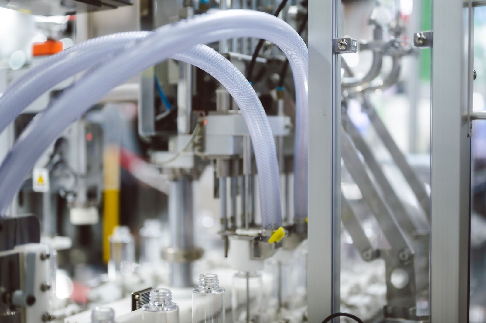
N-type monocrystalline silicon wafers are among the most advanced materials used in the semiconductor and solar energy industries. Known for their exceptional purity, high efficiency, and superior electrical properties, these wafers play a vital role in manufacturing integrated circuits, photovoltaic (PV) cells, sensors, and electronic devices. As demand for renewable energy and high-performance electronics continues to grow, n-type monocrystalline silicon wafers have become the preferred choice for manufacturers seeking reliable and long-lasting performance.
This guide explains everything you need to know about n-type monocrystalline silicon wafers, including their manufacturing process, advantages, applications, specifications, and factors to consider when choosing the right supplier.
Table of Contents
- What Are N-Type Monocrystalline Silicon Wafers?
- How N-Type Monocrystalline Silicon Wafers Are Manufactured
- Key Characteristics of N-Type Monocrystalline Silicon Wafers
- Benefits of Using N-Type Monocrystalline Silicon Wafers
- Applications Across Industries
- N-Type vs. P-Type Silicon Wafers
- Important Specifications to Consider
- Quality Standards and Testing
- Choosing the Right Supplier
- Future Trends in N-Type Monocrystalline Silicon Wafers
- Frequently Asked Questions
- Conclusion
What Are N-Type Monocrystalline Silicon Wafers?
N-type monocrystalline silicon wafers are thin slices of high-purity single-crystal silicon that are doped with donor elements such as phosphorus or arsenic. These dopants introduce extra electrons into the silicon lattice, making electrons the primary charge carriers.
Unlike polycrystalline wafers, monocrystalline wafers are made from a single continuous crystal structure. This uniform crystal arrangement minimizes defects, improves electrical conductivity, and enhances overall performance.
These wafers are widely used in:
- Solar photovoltaic cells
- Semiconductor chips
- Power electronics
- Microprocessors
- Sensors
- MEMS devices
- Research laboratories
- Advanced electronic components
Their high efficiency and reliability make them essential for modern technology.
How N-Type Monocrystalline Silicon Wafers Are Manufactured
The production of n-type monocrystalline silicon wafers requires precision engineering and strict quality control.
Silicon Purification
Raw silicon is refined into ultra-high-purity electronic-grade silicon to remove impurities.
Crystal Growth
The purified silicon is melted, and a single crystal is grown using methods such as the Czochralski (CZ) process or the Float Zone (FZ) process.
Doping
Phosphorus or another donor element is added during crystal growth to create the n-type electrical characteristics.
Ingot Shaping
The crystal ingot is ground into a uniform cylindrical shape with precise dimensions.
Wafer Slicing
Diamond wire saws cut the ingot into thin wafers with consistent thickness.
Surface Polishing
Chemical and mechanical polishing produce an ultra-smooth surface suitable for semiconductor fabrication.
Inspection
Each wafer undergoes testing for thickness, flatness, resistivity, crystal defects, and surface quality before shipment.
Key Characteristics of N-Type Monocrystalline Silicon Wafers
Several features make n-type monocrystalline silicon wafers ideal for demanding applications.
High Purity
Minimal contamination ensures excellent electrical performance.
Excellent Carrier Lifetime
Long electron carrier lifetimes improve efficiency in solar cells and semiconductor devices.
Low Impurity Levels
Reduced metallic impurities increase reliability and device lifespan.
High Mechanical Strength
These wafers resist cracking during manufacturing and processing.
Uniform Crystal Structure
The single-crystal lattice reduces grain boundaries and electrical losses.
Superior Thermal Stability
They perform reliably under varying operating temperatures.
Benefits of Using N-Type Monocrystalline Silicon Wafers
There are many reasons manufacturers prefer n-type monocrystalline silicon wafers.
Higher Energy Efficiency
Solar cells made from n-type wafers often achieve higher conversion efficiencies than conventional p-type cells.
Lower Light-Induced Degradation
N-type silicon is less susceptible to light-induced degradation, helping maintain long-term performance.
Longer Device Lifespan
Reduced impurity-related defects improve durability and reliability.
Better Electrical Performance
High carrier mobility supports faster and more efficient electronic devices.
Greater Resistance to Contamination
N-type wafers are less affected by certain impurities that reduce device efficiency.
Improved Manufacturing Yield
Their consistent crystal quality helps manufacturers achieve higher production success rates.
Applications Across Industries
N-type monocrystalline silicon wafers are used in many advanced technologies.
Solar Energy
High-efficiency photovoltaic panels increasingly use n-type wafers to maximize energy output.
Semiconductor Manufacturing
Microprocessors, memory chips, and integrated circuits rely on high-quality silicon wafers.
Power Electronics
Power devices require excellent conductivity and thermal performance.
MEMS Technology
Micro-electromechanical systems depend on precision silicon wafers for accurate performance.
Optical Devices
Certain photonic and optical components use monocrystalline silicon substrates.
Research and Development
Universities and laboratories use these wafers for material science and semiconductor research.
N-Type vs. P-Type Silicon Wafers
Understanding the differences helps manufacturers select the right material.
| Feature | N-Type Wafers | P-Type Wafers |
| Dopant | Phosphorus | Boron |
| Charge Carrier | Electrons | Holes |
| Light-Induced Degradation | Very Low | Higher |
| Solar Efficiency | Higher | Good |
| Carrier Lifetime | Longer | Shorter |
| Cost | Slightly Higher | More Affordable |
Although p-type wafers remain common, n-type monocrystalline silicon wafers are increasingly favored for premium solar and semiconductor applications.
Important Specifications to Consider
Before purchasing n-type monocrystalline silicon wafers, evaluate several technical specifications.
Diameter
Common wafer sizes include:
- 100 mm
- 150 mm
- 200 mm
- 300 mm
Thickness
Thickness varies according to manufacturing requirements.
Resistivity
Different electronic applications require specific resistivity ranges.
Crystal Orientation
Typical orientations include:
- <100>
- <111>
Surface Finish
Available finishes include:
- Polished
- Double-side polished
- Epitaxial-ready
- Lapped
Flatness
High flatness improves photolithography accuracy during semiconductor fabrication.
Quality Standards and Testing
Leading manufacturers perform extensive quality testing on n-type monocrystalline silicon wafers.
Common inspection methods include:
- Surface defect analysis
- Thickness measurement
- Flatness testing
- Resistivity verification
- Crystal orientation inspection
- Particle contamination testing
- Optical inspection
- Mechanical strength evaluation
Strict quality control ensures consistent performance throughout production.
Choosing the Right Supplier
Selecting a reliable supplier is essential for obtaining premium n-type monocrystalline silicon wafers.
Manufacturing Experience
Choose suppliers with extensive expertise in semiconductor materials.
Quality Certifications
Look for manufacturers certified under recognized international quality standards.
Customization Options
Many applications require custom wafer dimensions, resistivity, or surface finishes.
Technical Support
Reliable suppliers provide engineering assistance throughout the purchasing process.
Consistent Production
Stable manufacturing processes ensure uniform wafer quality across large production batches.
Global Distribution
Suppliers with efficient logistics help minimize delivery delays.
Future Trends in N-Type Monocrystalline Silicon Wafers
The future of n-type monocrystalline silicon wafers continues to evolve with technological innovation.
Emerging trends include:
- Higher-efficiency solar cells
- Thinner wafer technology
- Advanced heterojunction solar cells
- TOPCon solar cell manufacturing
- Improved crystal growth techniques
- Lower manufacturing costs
- Greater adoption in electric vehicle electronics
- Expanded semiconductor applications
As renewable energy demand increases, n-type wafers will continue to play a central role in next-generation technologies.
Frequently Asked Questions
What are n-type monocrystalline silicon wafers?
They are single-crystal silicon wafers doped with phosphorus or similar elements, making electrons the primary charge carriers.
Why are n-type wafers preferred for solar panels?
They offer higher efficiency, lower light-induced degradation, and longer operational lifespans compared to many p-type alternatives.
Which industries use these wafers?
They are widely used in solar energy, semiconductor manufacturing, MEMS devices, power electronics, and research laboratories.
What crystal orientations are commonly available?
The most common crystal orientations are <100> and <111>, depending on the application.
Are n-type wafers more expensive?
Yes, they generally cost more than p-type wafers because of their advanced manufacturing process and higher performance.
What factors should I consider when selecting a supplier?
Evaluate product quality, certifications, manufacturing experience, customization capabilities, technical support, and delivery reliability.
Conclusion
N-type monocrystalline silicon wafers represent one of the most advanced materials available for semiconductor and photovoltaic manufacturing. Their exceptional purity, high carrier lifetime, superior electrical performance, and excellent long-term stability make them the preferred choice for high-efficiency solar cells, integrated circuits, and advanced electronic devices. By selecting high-quality wafers from a trusted supplier and understanding the key technical specifications, manufacturers can improve production efficiency, enhance device performance, and support innovation across multiple industries. As renewable energy and semiconductor technologies continue to advance, n-type monocrystalline silicon wafers will remain a critical foundation for future technological progress.